Systems operating at >100 GHz tend to be based upon individually fabricated components, such as waveguide mounting structures, which are difficult and expensive to make. This has tended to limit the range of submillimetre-wavelength applications to highly specialised ones such as astronomy and atmospheric remote sensing. Mass market applications, including telecommunications require the use of more cost-effective technology.
Much of our work involves micromachining --- the use of microfabrication methods such as etching, photolithography and electroforming to manufacture not just high frequency devices, but also the embedding structures in which they are mounted. Such methods (a) provide a cost-effective means of fabricating high frequency components, and (b) permit fabrication of structures that might otherwise be impossible to produce.
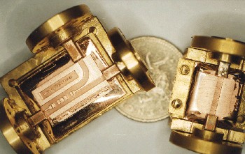
Our micromachining methods are used to fabricate integrated waveguide structures up to 2 mm in height. The image on the left shows a micromachined, resonant cavity waveguide filter (with lid removed). The structure consists of a bandpass waveguide filter, H-plane waveguide transformer (300 GHz to 600 GHz) and moveable tuning shorts. The irises forming the filter have widths of ~ 40 microns and heights of ~ 400 microns.